Designing your own STM32F103 PCB gives you full control over hardware — compact, power-efficient, and ready for production.
This complete guide walks through how to design and flash your custom STM32F103 board, finishing with an LED blink test using STM32CubeIDE and ST-Link V2.
Required Tools and Components
Hardware
- STM32F103C8T6 (LQFP48 package)
- 8 MHz crystal + 20pF capacitors
- 3.3V regulator (RT9193-33GB or AMS1117-3.3)
- LED + 330Ω resistor
- 10kΩ resistors (BOOT0, RESET)
- SWD 4-pin header
- Breadboard wires or PCB connectors
- ST-Link V2 programmer
- USB-to-UART module (CH340, CP2102, or FTDI)
- Multimeter, soldering tools, USB cable
Software
- STM32CubeIDE – Create, edit, and compile STM32 firmware
👉 Download STM32CubeIDE - STM32CubeProgrammer – Flash firmware to MCU
👉 Download STM32CubeProgrammer
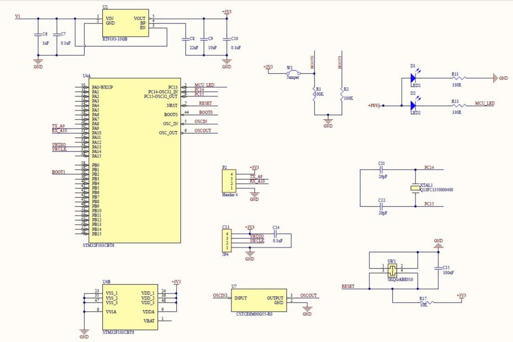
Step 1: Design the Core STM32F103 Circuit
The minimum working system for STM32F103 includes:
| Function | Pin(s) | Description |
|---|---|---|
| Power | VDD, VDDA | +3.3V from regulator |
| Ground | VSS, VSSA | Common ground |
| Clock | OSC_IN, OSC_OUT | 8MHz crystal + capacitors |
| Reset | NRST | 10kΩ pull-up + reset button |
| Boot | BOOT0 | Jumper to GND (Flash) / 3.3V (Bootloader) |
| SWD | PA13, PA14 | Programming via ST-Link |
| LED | PC13 | User LED |
| UART | PA9 (TX), PA10 (RX) | Debug communication |
Step 2: Power Supply and Voltage Regulation
Use RT9193-33GB LDO regulator (as in your circuit):
- Input: 5V (from DC adapter)
- Output: Stable 3.3V
- Capacitors:
- Input: 1µF
- Output: 10µF
- Connect 3.3V to all VDD and VDDA pins
- Connect GND to all ground pins and planes
Step 3: Add Programming Debug Interfaces
Add a 4-pin header to connect the ST-Link V2:
| Pin | Signal | Description |
|---|---|---|
| 1 | 3.3V | Power reference |
| 2 | SWDIO | Serial Wire Data |
| 3 | SWCLK | Serial Wire Clock |
| 4 | GND | Ground |
BOOT0 should be tied to GND for normal operation.
Keep the SWDIO and SWCLK traces short (under 5 cm).
UART (Debugging)
Add a 3-pin header for UART communication:
| Pin | Signal | Description |
|---|---|---|
| 1 | TX (PA9) | Connect to USB-UART RX |
| 2 | RX (PA10) | Connect to USB-UART TX |
| 3 | GND | Ground common |
You can connect this header to a USB-to-UART adapter (like CH340 or FTDI) for serial debugging in tools like PuTTY or Tera Term.

Step 4: PCB Layout Guidelines
- Keep the crystal and capacitors close to the MCU pins
- Place decoupling capacitors near every VDD pin
- Maintain a solid GND plane on the bottom layer
- Keep SWD and UART headers accessible on the board edge
- Place BOOT0 jumper and RESET button in easy reach
- Route TX/RX traces short and avoid noisy areas
Recommended Components
- MCU: STM32F103C8T6 (LQFP48)
- Crystal: 8MHz ±20ppm
- Regulator: RT9193-33GB
- Capacitors: 0.1µF × 4, 1µF × 1, 10µF × 1
- Resistors: 10kΩ (Reset, Boot0), 330Ω (LED)
Step 5: Generate Gerber Files
When your schematic and layout are done:
- Run DRC (Design Rule Check)
- Generate Gerber files (Top/Bottom Copper, Silkscreen, Solder Mask, Drill)
- Export BOM (Bill of Materials)
- Upload to a PCB manufacturer such as:

Step 6: Flashing Firmware (LED Blink)
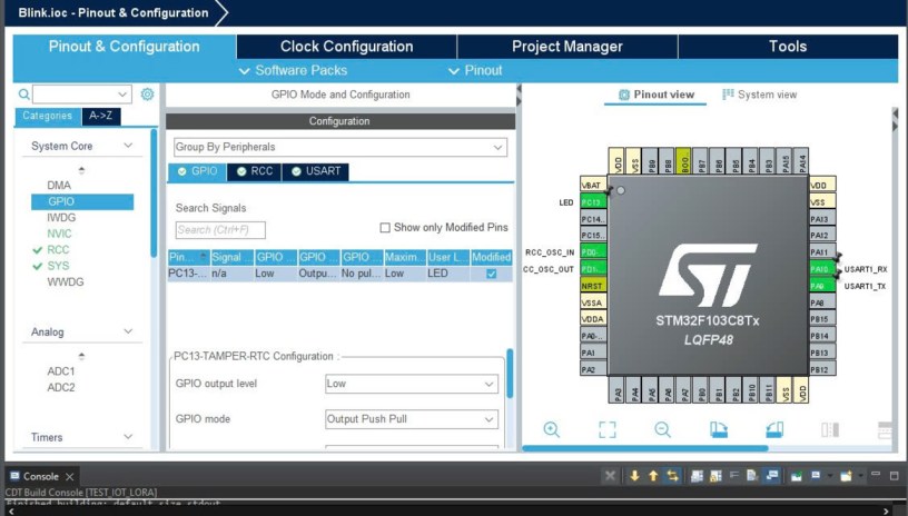
Open STM32CubeIDE → Create new STM32 project (STM32F103C8Tx) → Enable:
PC13as GPIO Output (LED)PA9/PA10as USART1 TX/RX (Asynchronous Mode, 9600 baud)
Replace main.c with this code:
#include "main.h"
#include "usart.h"
#include "gpio.h"
#include <stdio.h>

int _write(int file, char *ptr, int len) {
  HAL_UART_Transmit(&huart1, (uint8_t*)ptr, len, HAL_MAX_DELAY);
  return len;
}

int main(void)
{
  HAL_Init();
  SystemClock_Config();
  MX_GPIO_Init();
  MX_USART1_UART_Init();

  printf("STM32F103 Custom PCB Initialized\r\n");

  while (1)
  {
    HAL_GPIO_TogglePin(GPIOC, GPIO_PIN_13);
    printf("LED toggled\r\n");
    HAL_Delay(1000);
  }
}
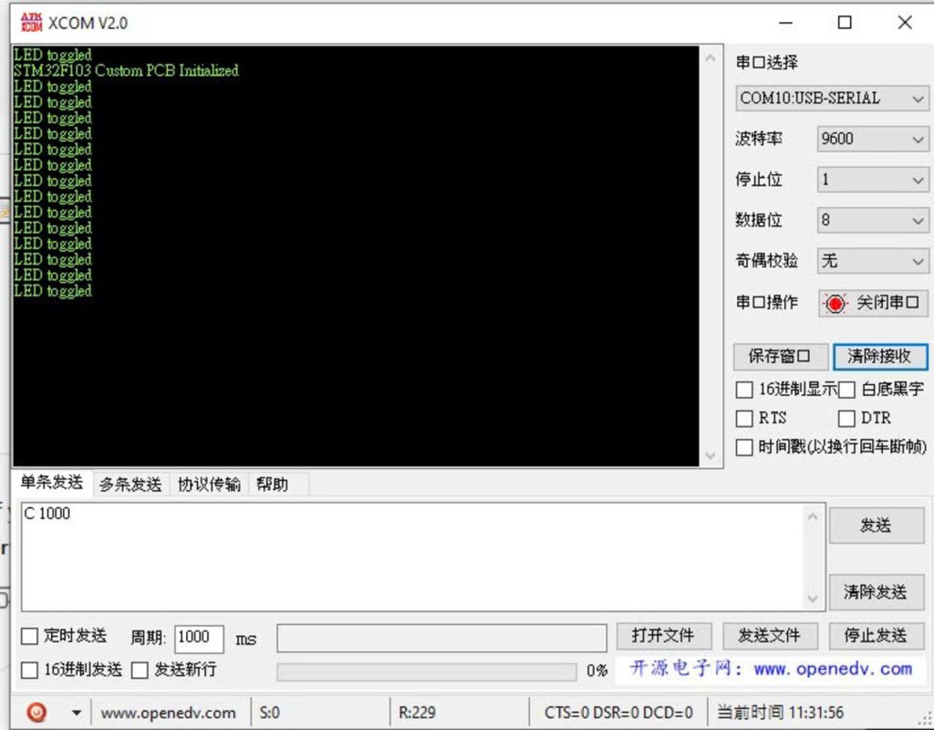
You can view UART output by opening a serial terminal (115200 baud, 8-N-1).

Step 7: Build and Upload
- Connect ST-Link and power up your board
- Click Run ▶ in STM32CubeIDE
- STM32CubeProgrammer flashes the firmware automatically
- Open your UART terminal — you should see:
STM32F103 Custom PCB Initialized
LED toggled
LED toggled
And your LED on PC13 blinks every 1 second 🎉
Troubleshooting
| Issue | Check |
|---|---|
| Flashing failed | Verify SWD connection and 3.3V power |
| No UART output | Check TX/RX orientation and baud rate |
| LED not blinking | Verify PC13 LED connection |
| MCU not detected | Ensure BOOT0 = GND and RESET high |
| No 3.3V | Inspect regulator (RT9193) and input voltage |
Step 8: Final Notes
You now have:
- A custom STM32F103 PCB
- ST-Link SWD programming interface
- UART debug capability (PA9/PA10)
- Working LED blink firmware
This foundation allows expansion to:
- I²C, SPI, and ADC sensors
- LoRa, BLE, or Wi-Fi modules
- Battery power and deep-sleep IoT designs
Project files on GitHub:
All design files, source code, and firmware for this custom STM32F103 PCB are available at the GitHub repository: github.com/Haipk001/Custom-STM32F1
Please make sure to download the latest files from the “Circuit” and “Core” folders before building or programming the board.
