In this article, I would like to share the results of my power-saving tests on a custom wireless sensor node using the ATMega328P. While I’m making progress, I’m still not entirely satisfied with the power consumption levels of my custom PCB. However, the results are promising, and I’m sharing my findings for those interested in optimizing power usage on their sensor nodes.
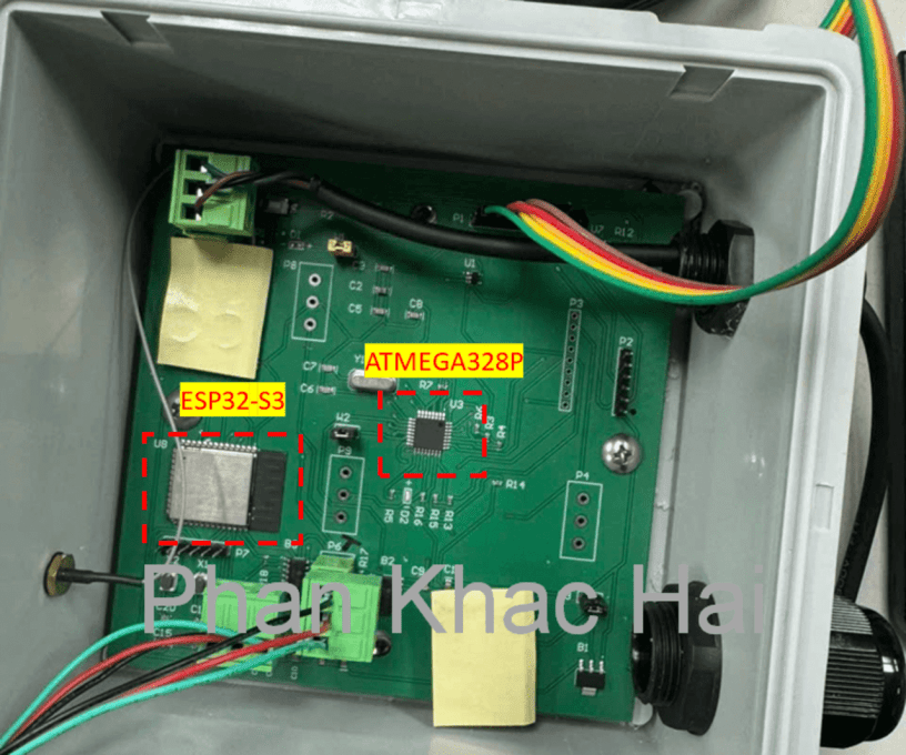
Overview of the Wireless Sensor Node
My wireless sensor node consists of two primary parts:
- ATMega328P as the main MCU.
- ESP32-S3 as the secondary MCU responsible for reading sensor data.
These two MCUs are connected via UART TTL for seamless communication. Below are the circuit designs for both components:
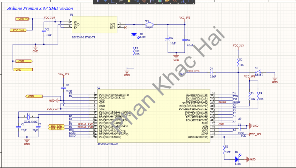
Figure 1: ATMega328P circuit design
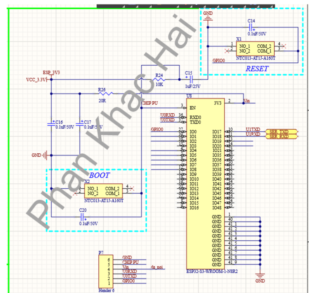
Figure 2: ESP32-S3 circuit design
Power Consumption Test Results
When testing the power consumption of my wireless node, I measured the following results:
- Deep Sleep Mode: The current consumption dropped to 1.29 mA.
- Active Working Mode: The current consumption was 6.42 mA.
Although these results show significant power savings in sleep mode, they still fall short of the ultra-low power consumption I was aiming for. For example, with an Arduino Pro Mini by SparkFun, the deep sleep mode consumption was a mere 0.2 mA. This huge difference indicates there is room for improvement in the current design.
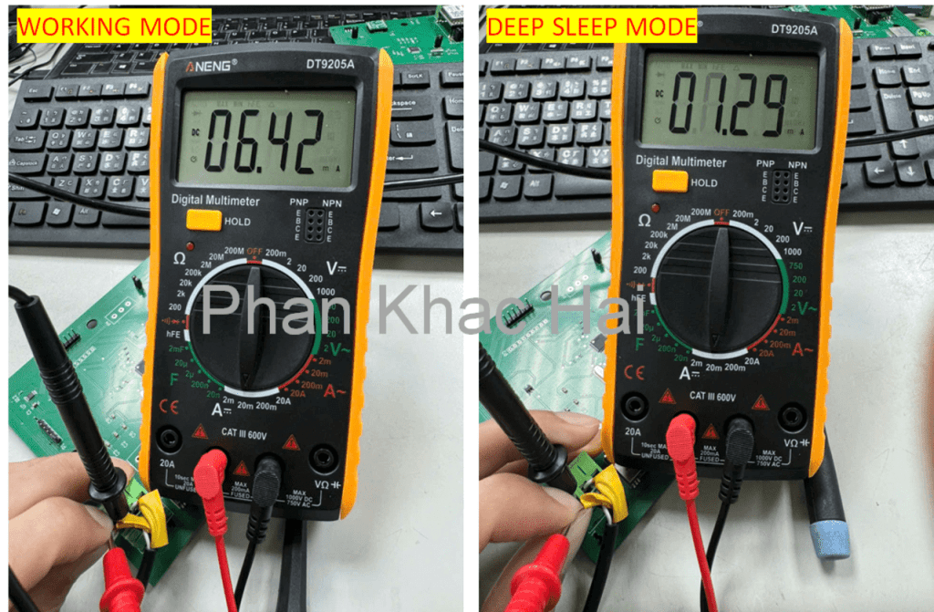
Figure 3: Power consumption comparison between deep sleep and active working modes.
Next Steps
To achieve better results, I plan to revise my circuit design and replace certain electronic components to minimize the current draw further. My goal is to reach power consumption levels similar to or better than the Arduino Pro Mini, which is well-known for its low power usage.
In conclusion, while the current version of the node has shown some improvement in power savings, there’s still a way to go in optimizing for minimal current draw. I’ll continue to work on improving the design and share updates as I progress.
Stay tuned for more on how to further optimize your sensor nodes for better power efficiency!
